
One would think that the title of this article should be a no-brainer. The fact of the matter is that the ownership of this vital aspect of electronic design is not only cloudy, but it will become murkier in the next 10 years. This murkiness is also an opportunity for mechanical engineers who aren’t afraid to expand their horizons.
In order to understand the current climate, we have to look at the division of labor that took place in electronic design about 40 years ago. The labor was divided into two processes, with the first being the design itself. This process was (and still is) owned by the electrical engineers.
Though circuit design has changed, the methods for representing the circuit have not. Electrical engineers were designing circuits with discrete components such as transistors, amplifiers, resistors, capacitors, diodes, etc. They did not concern themselves with the physical details. They would call out values and key characteristics of the components. All of this design was and still is represented in an abstract form, meaning, the components are drawn using symbolic representations and the schematic drawings are dimensionless.
Electrical engineers were back then and are still taught circuit design theory. Granted, a good university program will demand some electronic lab classes; however, it is all done on proto boards to prove out some concept. What one will rarely find in a university classroom is a PCB design course. The only time an electrical engineering student will be exposed to a PCB is if he signs up for a senior project that requires the creation of a PCB.
The second step of the design process is the layout of the physical board. It was rare for the electrical engineer to layout the PCB. Once they were done with the circuit design, this was handled off to a layout artist. A layout artist may have gone through a technical school, but in many cases, they were tech-savvy individuals out of high school. They made the decisions as to how the schematic was to be represented in real life. It was an art form using Mylar and tape.
Throughout the 1970s, the integrated circuit (IC) chip became more prevalent. The functionality that was created by individual discrete components could now be etched in silicon and take up a space that was far smaller. This may have reduced the real estate used on the board for discrete components, but now there were more component pins to route in a small space.
By the mid-1980s, the Mylar and tape method of board layout was becoming a difficult process. The electrical engineers were not designing with discrete components, rather, they were designing with ICs. This required more than two layers of copper on the PCB. To remedy this, computer programs were developed to assist in the layout of the PCB. The layout artists traded their light tables for desktops with electronic design automation (EDA) tools.
Since the 1980s, the PCB layouts have become more complex. More so, it is very safe to say that the PCB is not going to go the way of the dinosaur. However, we have to recognize that the three economic downturns in the last 30 years have had a monumental impact on PCB layout artists. The first was in 1990, followed by the tech wreck in 2001 and the great recession of 2008. In each of the subsequent recoveries, the burden of PCB layout has been put on the shoulders of the electrical engineer. In fact, PCB layout is now a line item in a job position for a hardware engineer.
Surveys by Mentor confirm this. What they have found is that over 75 percent of those who call themselves layout artists are over the age of 45 (as of 2017). More importantly, other surveys indicate that 50 percent of them plan to retire within 10 years.
What does this mean?
- Those who are layout artists have had a tough row to hoe. They have survived three major downturns. They know that if they were passing their information to someone else, they are threatening their own existence. They have no incentive to teach a new generation.
- Academia still looks at the layout as a technician’s job. Therefore, they do not see the need to teach this skill to their engineering students. Academia is completely out of touch with the industry.
- No vocational program really exists to train individuals on PCB layout.
- As mentioned, PCB is not going away any time soon. It is vital medium for electronic design.
- Mechatronic design is going to lean heavily on the concepts that are currently use in PCB layout. Understanding the current methods used to design and fabricate a PCB will be necessary for mechatronic manufacturing methods.
As the title suggests, we in the PCB design space do not have someone to take ownership of the layout. There is no effort in the industry to replace or recreate the position of layout artist. The electrical engineering community has not embraced it because most of the focus is on component development and embedded programming. They are still trained in theoretical concepts of circuit design. Few venture into the physical hardware.
In thinking outside the box, the PCB is just as mechanical as it is electrical. We at Nine Dot Connects have made it clear that mechatronic design is the simultaneous blending of both the mechanical and electrical. When we really look at the PCB, it just as much mechanical as it is electrical. In fact, it is bold to say that the PCB itself is truly a mechatronic design. When the layout artists are designing a PCB, they are considering both the electrical and mechanical aspects simultaneously.
Therefore, who’s to say that the PCB cannot be owned by the mechanical? In a blog post to come, we will explore the reasons why a mechanical engineer can own this space, a space that will only become more precious as time moves on.
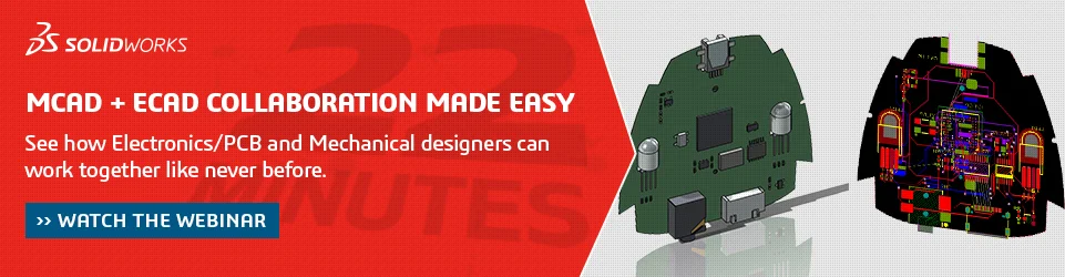
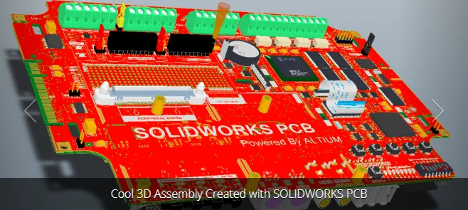
Find out how you can unite your mechanical and electrical design teams with integrated tools from SOLIDWORKS by clicking on the banner below. Also, keep an eye out for Part 2 of Who Really Owns the PCB Layout coming next week.