This article’s argument for mechanical engineering involvement in PCB design is specific to the layout. The schematics and circuit design such as power, analog, and digital belong to the electrical engineering domain and this area requires classroom and lab experience which one would expect from a degreed electrical program. It is not to say that a mechanical engineer cannot do circuit design. More so, we envision a future in which academia offers degrees in mechatronic design. Under the current circumstances, this industry is notorious for making gross assumptions about an engineer’s capabilities, and we wish not to propagate the belief that a mechanical engineer can do the whole PCB design based on their degree alone unless they have been exposed to circuit design during their undergraduate career.
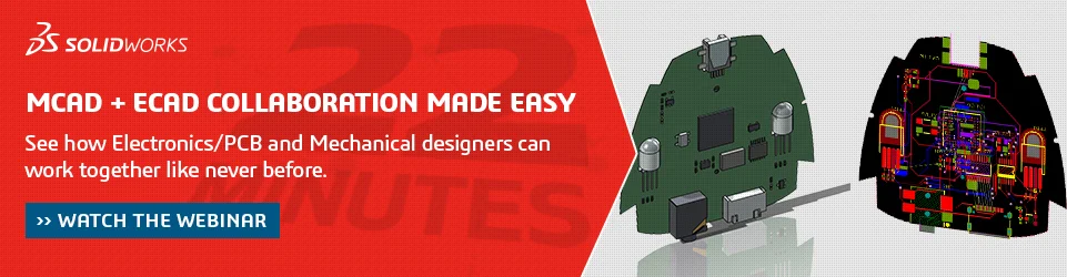
In our last blog post, we made the bold statement that the PCB layout is just as much a mechanical effort as it is an electrical one. We can go so far as to say that the PCB is an excellent example of mechatronics, the simultaneous blending of electrical and mechanical design practices. In this article, we will make the argument that it may be the mechanical engineers who are more prepared to take on the PCB layout.
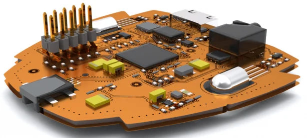
Library Development – One of the critical aspects of the layout is the creation of the footprint. The footprint is the exposed copper on the board which will be used to attach the component during the assembly process. For the leads of the component to be fitted properly to the board, the pads of the footprint must be dimensioned to accommodate tolerances. Notice the words ‘dimensioned’ and ‘tolerances’ in the prior sentence. This is not the vocabulary of an electrical engineer nor is it something that an electrical engineer would be taught in an undergraduate program. Yet, any draftsman or mechanical engineer would be familiar with these terms.
The Institute of Electrical and Electronic Engineers (IEEE ) and IPC (Association Connecting Electronics Industries – yes, their name does not match their acronym) are the two primary ‘authorities’ of the electronics industry. What is surprising is that when it comes to PCB specifications, handbooks and even the IPC’s Certified Interconnect Designer (CID) program, these documents are steeped in mechanical requirements. The IPC CID certification is focused on the requirements necessary to design a PCB that is manufacturable. In 2013 version of the CID training, Geometric Dimensioning and Tolerance (GDT) was introduced in depth. GDT is not taught to an electrical engineer unless he or she goes out of the way to learn it.
Beyond the footprints, there are also 3D component shapes. The ability to add these components to the footprints in the ECAD tools has greatly aided in the ability for the PCB board to be fitted based on 3D representations. The mechanical folks have been instrumental in making these components available. In a sense, mechanical engineers currently play a bigger role in the creation of footprints than they may realize.
Board Shape – We can no longer ignore the impact that marketing has on the shape of board. In many cases, the look of the product comes from the marketing department. Since the look of the product is mechanical in nature, they are inclined to interface with the mechanical team to bring their idea into a 3D representation. As a result, the board shape is being influenced by an organization that knows nothing about engineering and one that is driving the mechanical team, which knows very little about electronics. Having a PCB-savvy mechanical team can go a long way in representing the needs of the circuit designers.
In the past, a square or rectangular board would have been adequate given the space available in the product’s mechanical enclosure. The design of the enclosure was based on the final product of the PCB layout. Advancements in the MCAD tools and manufacturing allow for products that are anything but square. Many board shapes are now being imported from the MCAD tools based on the dimensions of the enclosures. It is not unusual to find board with asymmetric curves. When it comes to complex shapes, MCAD tools are far better suited for drawing a board outline than the ECAD tools. In some EDA tools, one can create a board shape based on an imported enclosure, but this enclosure was more than likely created in an MCAD tool.
Component Placement – Component placement has been another area that is becoming more driven by the mechanical design. It is now commonplace to pass the board and its components between the ECAD and MCAD tools. This is imperative to check key locations, especially components that the end user will need to press, such as a button or a switch, a display monitor or LEDs, or connect through a cable. The mechanical designer (and even the marketing team) have just as much input on the component placement as does the layout artist.
Through this collaboration, both the electrical and mechanical aspects of component placement may be sorted and determined prior to routing. This is a great example of mechatronic design in action, for it considers both the electrical and mechanical needs in real time. Without this collaboration, high-profile components are overlooked, and fitment conflicts between the board, the components, and the enclosure are prevalent.
Rules Checker – The PCB editor is driven by a rule checker. This includes, but certainly not limited to, copper clearances, component clearances, trace widths, via sizes, and copper pull backs. Like the footprints, these rules are driven by tolerances and dimensions. Though some of these are also driven by electrical requirements especially in power or high-speed design, most of these rules are declared to ensure that the board can be fabricated and assembled. This again goes back to the commentary above about the need to understand GDT.
Routing – One of the biggest challenges of the design is the routing of the copper. This is one of those areas that requires experience and innate skills. It is certainly not taught and even if it was, the curriculum would be based on “rules of thumb” and constant exercises to hone the skills. Therefore, no single engineering discipline may lay claim to being best at routing.
Note that ECAD tool developers recognize the time and effort required to route boards. Because of market competition, there is an ongoing push to provide more features and tools to automate the routing and/or to assist in trace placement. Regardless, autorouting requires the layout artist to have a defined strategy, and that still requires experience and skills.
Thermal – Thermal issues have always been a concern with PCBs, especially in harsh environments and circuits with power components. With high speed design, thermal issues also have a major impact on the Power Distribution Network (PDN) of the board. Both ECAD and MCAD have been responding to this need with simulation tools. Most simulation tools require the user to provide initial conditions, meaning the user must have a fundamental understanding of heat flow. Like other aspects of the PCB design, thermal dynamics tends to be taught in mechanical engineering.
Conclusion
The point of this discussion is to show that the PCB is as much a mechanical design as it is electrical. Granted, there are PCBs that are so complex that they do need the experience and knowledge of an electrical engineer; however, the PCB layout is very much a mechanical creature that can be tackled by a mechanical engineer with a bit of knowledge and experience of the ECAD tools and the overall design process.
More so, we are seeing that the PCB is truly a mechatronic design. It needs to be designed with both electrical and mechanical needs in mind. As one looks to the future, we can no longer turn a blind eye to 3D printing, conductive inks, and embedded components. The way we fabricate and assemble electronics will not only be very different, the skill sets will also be different.
At Nine Dot Connects, we see a critical need for designers to get involved with the design of PCBs, regardless of their degree or experience. If you are looking to understand more, contact us. We provide tools, and more importantly the training, so these valuable skills can be learned before making mistakes that cost money and time. More importantly, these skills will prepare you for the next generation of design.