
It may surprise you to know that it is the exception to find an electronic device that does not have a printed circuit board (PCB). Every device around you has one. There’s a bigger picture to consider when comes to the PCB, especially as we enter the age of mechatronics. The purpose of the PCB has changed over time and its role in mechatronics is going to be very important.
PCBs started off as nothing more than a convenient way to organize components. As the components got smaller with more pins, the PCB was improved to allow copper to connect between the components without having to solder individual wires. As the pin counts on these components grew, there came the ability to design boards with multiple layers of copper to handle all of the signaling. In this age of high-speed design, one cannot build such circuitry without the physical structure of the PCB to assist.
In fact, all of the other electrical engineering disciplines, whether it be chips and components, Radio Frequency (RF), system, and even fiber optic, require the PCB to assist in bringing it all together. It is fair to say that the PCB is the electronic medium of all electronic mediums.
In the 1990s, there was a revolution of sorts in the design of computer chips (commonly referred to as ASICs). Moore’s law stated that the number of transistors one could put on a chip was doubling every one to two years. In the 1990s, this technology hit the knee curve of the law, thus bringing the technologies that we enjoy today, such as computers, cell phones, and the internet. Oddly, there was also a lot of talk about the PCB becoming a relic of the past. The idea was that silicon would become the new electronic medium.
As it turned out, this did not come to fruition and more so, the PCB is as important now as it has ever been. The chips of today have to communicate with the outside world and the PCB provides this avenue. As mentioned easier, customers expect high-speed responses. The physical forces in play require the structure of the PCB to make this possible.
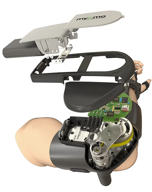
Now with the advent of mechatronics becoming a reality, the PCB is going to take on another role. In addition, to being a component holder, a copper connectivity device, and a structure for high-speed signaling, it is now poised to be an integral part of the mechanical design. Currently, PCBs are integrated into the mechanical housings. Mechatronics demands that the PCB is just as much as part of the mechanical structure as it is electrical. Consider the arm of a robot. Currently, we create the arm through mechanical CAD tools and the control of the arm through electrical EDA tools. We then integrate this by accommodating the PCB in the mechanical and then run wires from the PCB to those areas that require the signaling. The PCB does not provide structural assistance; rather, the mechanical protects the PCB.
The mechatronics view of the world sees the PCB as part of the structure of the arm along with the controls. More so, the develop of the PCB accommodates the electrical and mechanical elements at the same time. The design interweaves the electrical with the mechanical.
Hopefully, this very brief introduction to PCBs gives you an idea of the importance this medium plays in electrical and mechanical engineering. There is no doubt that the next wave of technology will come from devices that provide both electrical and physical capabilities. This is going to be an opportunity for those embrace the concept of mechatronics and a bane for those who continue to treat the PCB as an ‘electrical’ thing.
If you’d like to know about this topic, watch the video titled “A Short History of the Printed Circuit Boards” created by Nine Dot Connects.
We’re going on the road…See if we are coming to your town for “The Rise of Mechatronics Roadshow.” See if we are coming to your town…